Cleanroom-Grade Smart Solutions for Semiconductor Manufacturing
For wafer fabrication, chip packaging/testing, and other semiconductor processes, we deliver cleanroom-compatible, ultra-high-precision, low-particulate, contamination-free smart end-effectors that meet Class 100/Class 10 cleanliness requirements and empower semiconductor automation.
Challenges in Semiconductor Manufacturing
Extreme Cleanliness Requirements
Semiconductor fabrication runs in cleanrooms, requiring end-effectors to be low-particulate, oil-free, and free of particle contamination — standards ordinary grippers cannot meet.
Sub-Micron Precision
Processes such as wafer alignment and die bonding require sub-micron positioning; the slightest deviation causes scrap at enormous cost.
Extremely Fragile Workpieces
Wafers are thin and brittle and chips are tiny, demanding extremely gentle force control; any slip causes cracks or chipping.
ESD & Contamination Control
Semiconductor devices are highly ESD-sensitive and must be protected from metal-ion contamination, imposing stringent material and surface-treatment requirements.
High Reliability Demands
Semiconductor equipment is highly valuable with costly downtime, demanding extreme reliability and high MTBF from end-effectors.
Industry Certification Requirements
Compliance with SEMI standards, CE marking, and other industry norms imposes strict material, design, and safety requirements.
Core Advantages of Jodell's Semiconductor Solutions
Cleanroom-Compatible
Designed to ISO Class 5 (Class 100) cleanliness with low-particulate materials, lubrication, and special surface treatment that do not contaminate the clean environment.
Ultra-High Precision
Rotation repeatability of ±0.005° and linear repeatability of ±0.01 mm meet high-precision wafer alignment and die bonding demands.
Ultra-Gentle Force Control
0.05 N force-control resolution enables ultra-gentle gripping of wafers and chips, preventing cracks and chipping and greatly improving yield.
ESD Protection
Anti-static surface treatment and grounding deliver ESD protection that meets semiconductor requirements, safeguarding devices from static damage.
Contamination-Free Materials
Semiconductor-grade materials are silicone-free and free of metal-ion contamination, suiting front-end processes such as wafer fabrication.
SEMI-Standard Design
Compliant with SEMI S2 safety standards and CE-marked, enabling direct integration into semiconductor tools with full-machine certification.
Typical Application Processes
Wafer Handling
Precision transport and loading/unloading of silicon and SiC wafers between process tools.
Wafer Alignment
Wafer notch alignment and rotary positioning; high-precision rotary stages guarantee alignment accuracy.
Die Pick & Place
Die bond pickup and placement with precise force control that does not damage the die.
Test & Sorting
Loading/unloading of chip test handlers with high-speed, accurate pick-and-place supporting parallel multi-station operation.
Wire Bonding
Precision positioning for packaging wire bonding with high-accuracy motion control.
Dispensing & Coating
Precise motion for packaging dispensing and underfill, with uniform bead volume and accurate positioning.
Real Application Demonstrations
Official demo videos from Jodell Robotics, showcasing end-effector performance in real production lines across industries.
LGBT Chip Mounting
LRA Motor Testing
LRA Linear Rotary Actuator
Recommended Products for Semiconductor
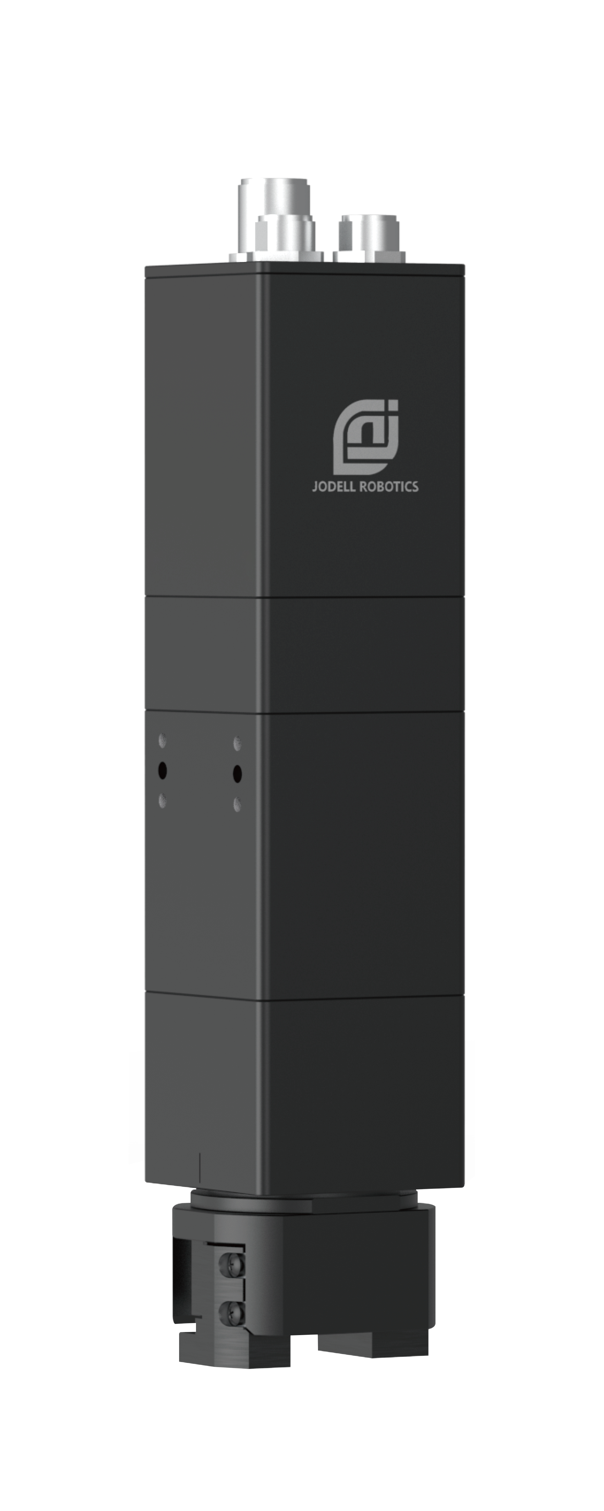
ERG-HP High-Precision Rotary Gripper
Ultra-high-precision rotation for wafer alignment
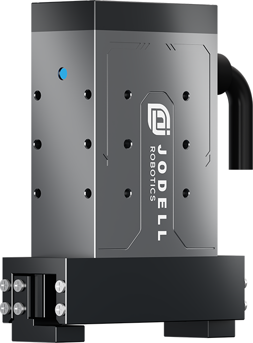
EPG-HP High-Precision Gripper
Sub-micron precision for die pickup
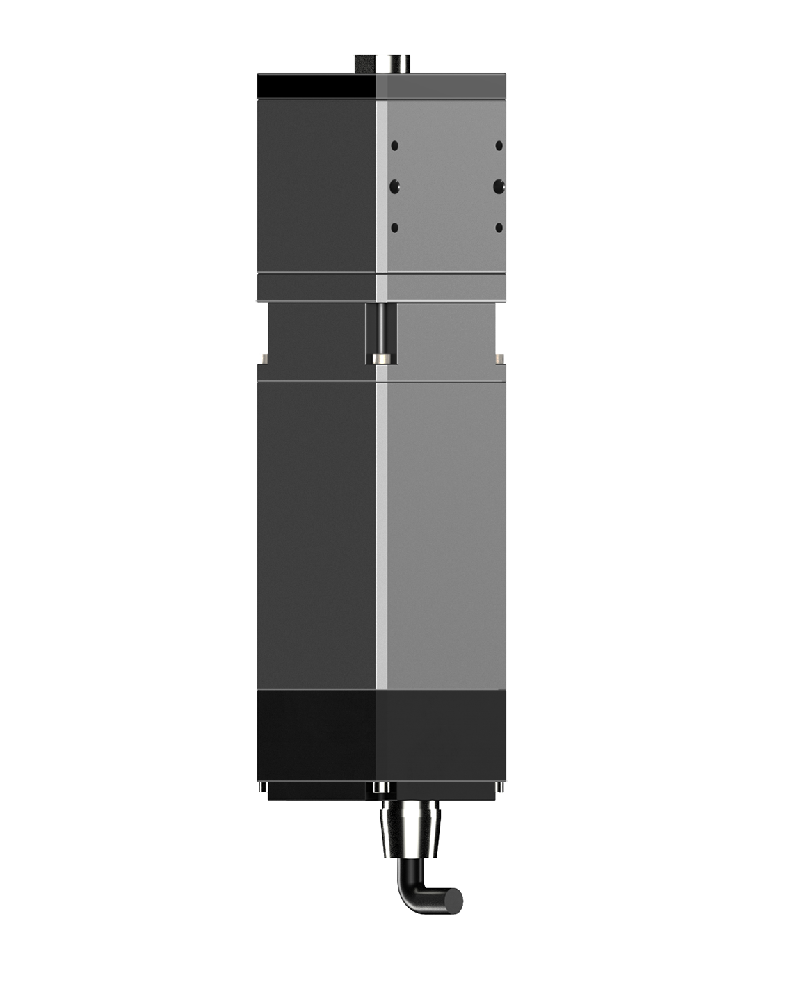
ERS Rotary Vacuum Actuator
Rotary vacuum for wafer handling
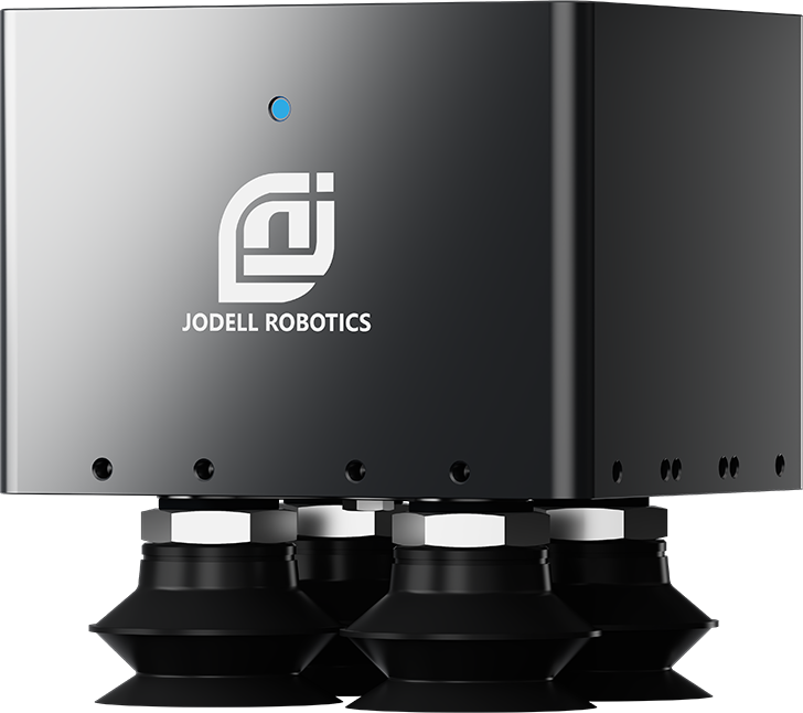
EVS Vacuum Actuator
Vacuum pickup for die handling
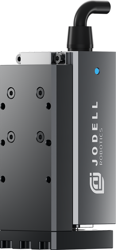
ELS Precision Linear Slide
Precise linear motion for dispensing positioning
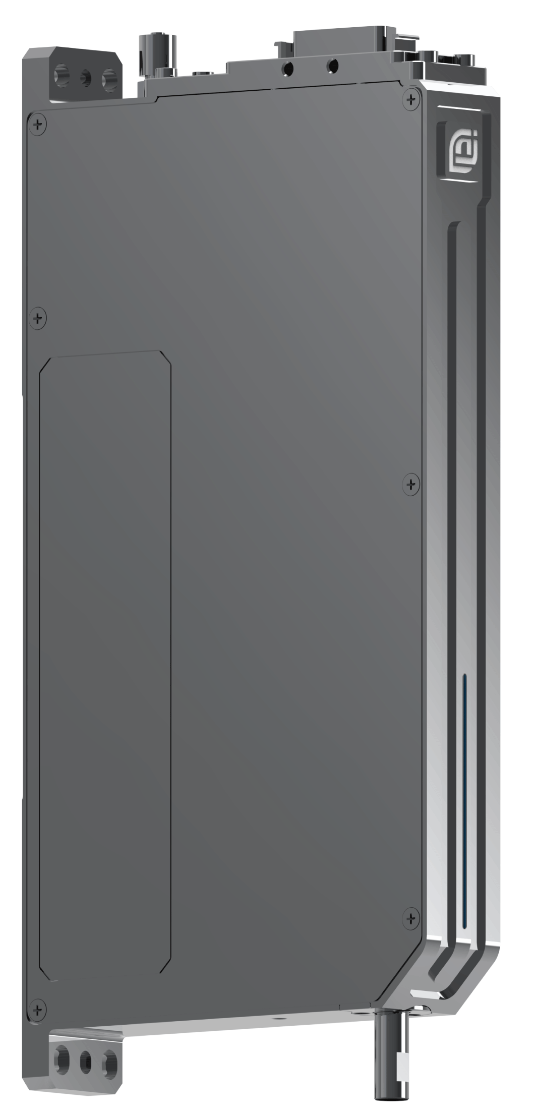
LRA Linear Rotary Actuator
Two-axis combo for precision fastening
Value We Deliver
Frequently Asked Questions
What cleanliness class do semiconductor grippers need to meet?
Cleanliness requirements vary by process: front-end wafer fabrication generally requires ISO Class 4-5 (Class 10-100), while back-end packaging/testing generally requires ISO Class 6-7 (Class 1000-10000). The Jodell ERG-HP series high-precision rotary gripper uses a dedicated cleanroom design with low-particulate lubrication and special surface treatment, reaching ISO Class 5 for front-end processes. The EPG-HP series reaches ISO Class 7 for back-end packaging and testing.
Why are vacuum actuators recommended for wafer handling?
Wafer surfaces are flat, smooth, and brittle, making vacuum pickup the standard approach for semiconductor wafer handling: 1) Bernoulli non-contact or soft contact does not damage front-side circuits; 2) Even vacuum force prevents wafer bending; 3) Edge or back-side contact avoids contaminating the wafer front. The Jodell ERS series rotary vacuum actuator maintains suction through 360° rotation, making it ideal for wafer alignment and handling.
How do semiconductor grippers address ESD?
Semiconductor devices are extremely sensitive to electrostatic discharge (ESD); even human-level static can destroy a chip. Jodell's dedicated semiconductor grippers address ESD in several ways: 1) Anti-static POM housing or anti-static coating with surface resistance of 10^6-10^9 Ω; 2) Dedicated grounding paths for fast static discharge; 3) Anti-static PEEK fingers; 4) Optional ionizing air nozzle port for further static elimination.
Can they be used on silicon carbide (SiC) wafers?
Yes. SiC wafers are a third-generation semiconductor material — hard but brittle and more difficult to process. The Jodell ERG-HP high-precision rotary gripper and ERS Rotary Vacuum Actuator are already deployed at multiple SiC device manufacturers for SiC wafer handling, alignment, and inspection loading/unloading, with precise force control and stable operation.
Do you offer semiconductor customization services?
Yes. Semiconductor tools vary widely, and standard products may not fully meet every need. Jodell provides customization based on specific requirements, including special materials (PEEK, PPS and other semiconductor-grade materials), special fingers (wafer-edge gripping, Bernoulli chucks), custom dimensions, and specialized communication protocols — supporting the full cycle from prototyping to mass delivery.
Get Your Dedicated Semiconductor Solution
Jodell Robotics brings deep semiconductor automation experience and delivers customized smart end-effector solutions for your tools.